Page 9 - Surface-Confined Assemblies and Polymers for Molecular Logic
P. 9
Surface-Confined Assemblies and Polymers de Ruiter and van der Boom


                                                               for the design of nonvolatile memory. The presented mem-
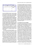
          TABLE 5. General Characteristics for Multistate Memory 40
                                                               ory is volatile (SRAM), and the information is eventually lost.
                                                               In this respect, the retention times of the PEDOT are excellent.
                                                               However, the propagation delay of PEDOT is only 500 ms,
                                                               which is a possible drawback for device performance, and
                                                               together with physical integration of molecular entities, are
                                                               commonly encountered bottlenecks in molecular logic.
                                                                  In the aforementioned examples, we demonstrated multi-
                                                               state memory that functions with I N inputs, where N is the
                                                               number of states (N =25). Their behavior can be described
                                                               bythe truth table shown inTable 5 and belongsto the flip-flop
          access memory (DRAM) that was able to reach four and five  family. These circuits contain at least two cross-coupled NOR
          states. This type of memory needs a periodical potential  gates that store the corresponding state. In our case, addi-
          pulse, typically in the millisecond regime, in order to maintain
                                                               tional OR gates are required to correctly convert the inputs I N
          the current state. The memory properties might be improved
                                                               to appropriateinputs forthe NORgates.For twocross-coupled
          by increasing the fwhm and the stability of the SPMA.
                                                               NOR gates, the flip-flop circuit is obtained, which is the main
            In our search for suitable materials and to expand the scope
                                                               constituent of static random access memory (SRAM). Increas-
          from molecular assemblies to polymers, we tested poly(3,4-  ing the memory state by one results in the functional integra-
          ethylenedioxythiophene) (PEDOT; Scheme 1C). 40  This electro-
                                                               tion of one extra NOR gate into the circuit (Figure 14).
          chromic polymer is robust and operates at low potentials,
                                                               Multistate molecular random access memory has attracted
          making it a suitable candidate for demonstrating multistate               41,42
                                                               much attention recently.
          memory. Similar to our monolayers and the SPMA, 32,37,38  we
          used here the optical absorbance as output signal (λ = 630 nm)
                                                               VI. Conclusions and Future Outlook
          and various potentials as inputs. Also in this material, the
          absorbance is a precise function of the applied potential. The  Molecular logic has seen rapid developments in the past few
          fwhm is considerably larger than that for SPMA (0.4 vs 0.17 V).  years (Figure 3), and important logic gates and circuits have
          Moreover, the observed E 1/2 is centered on 0.01 V, which  been demonstrated. 1122  Proof-of-principles and some ap-
          ensures that a future device might work at a low power  plications of molecular logic have been introduced. 1215,35
          consumption. The good stability of the PEDOT, combined with  Nevertheless, interesting and difficult challenges remain,
          a favorable fwhm, resulted in excellent retention times and,  including (i) a decrease in the propagation delay, (ii) homo-
          moreover, enabled us to demonstrate multistate memory  genization of the input and outputs, (iii) physical integration
          beyond ternary.                                      of logic gates, (iv) increasing the fan-out, and (v) solid-state
            For example, the use of four input potentials (i.e., 0.60,  logic gates/circuits. The propagation delay is an essential
          0.10, 0.15, and 0.60 V) generates four distinct absorption  figure-of-merit, because an input should remain active with-
          values that represent the four states in the memory  in this time frame. If an input change does occur, an error
          (Figure 12A). In addition, the memory could be expanded  during the data processing/storage is introduced. For many
          to quinary memory by adding a potential value at 0.00 V  chemical addressable logic gate/circuits, this propagation
          (Figure 12B). One might expand the number of states,  delay is in the order of minutes, which constitutes a bottle-
          provided that the ΔA of the absorption is sufficient; however,  neck. For our electrical addressable flip-flops, we were able
          this would not be beneficial because the gain in efficiency  to reduce this delay to ∼180 ms, which is a step toward real-
          (cost) decreases by incrementing the radix to a large extent.  world applications. 38  It would beneficial to use entirely
            The input potentials can be reconfigured to increase the  optical or electrical addressable logic gates/circuits. They
          retention times of quaternary and quinary memory. The  have been shown to exhibit small propagation delays
          absorbance values are particularly stable between 0.00 and  and have homogeneity between input and outputs, which
          0.60 V.Therefore, choosing the fourand five potentialswithin  allows for the possible concatenation of logic gates.
          this range resulted in retention times of 60 min for the  To achieve concatenation of logic gates, it is important
          quaternary memory and 20 min for the quinary memory  that the inputs and the outputs are homogeneous. Redox-
          (Figure 13). These retention times approach the range needed  active films are of particular interest, as it was shown that


                                                                   Vol. 44, No. 8 ’ 2011 ’ 563–573 ’ ACCOUNTS OF CHEMICAL RESEARCH ’ 571

