Page 2 - Molecules for Charge-Based Information Storage
P. 2
Molecules for Charge-Based Information Storage Lindsey and Bocian


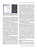
                                                               and one capacitor (Figure 1). Charge stored on the capacitor
                                                               indicates the bit level (either 0 or 1). To store sufficient charge
                                                               (∼200000 electrons) for accurate readout, a trench (or stack)
                                                                                    2
                                                               type capacitor is utilized. These designs lead to extremely
                                                               high aspect ratios, which are not easily scalable to the smallest
                                                               feature sizes now achievable via lithography (∼20 nm).
                                                                  Another disadvantage arising from the small dimensions
                                                               of the transistor gate in the DRAM cell is that the charge on
                                                               the capacitor decays rapidly (tens of milliseconds in current
                                                               constructs) via a leakage current through the transistor.
                                                               Thus, the data stored in each memory location must be
          FIGURE 1. Trench capacitor. Conceptual illustration showing crossbars  periodically refreshed by reading it out and then writing it
          (red, blue), transistor, and trench capacitor (left). Image of a 78-nm trench  back again. The frequency at which this refresh must be
          DRAM cell (with 70:1 aspect ratio) showing numerous trenches (right).
                                                               repeated is determined by the magnitude of the capacitance
                                                               and the leakage current; thus, a key design feature in the
          electronic properties over a broad range through molecular  miniaturization of DRAM cells is the available capacitance as
                                     1
          design and chemical synthesis. However, the molecular  the feature size shrinks. If DRAM cells could reach the same
          components employed must remain robust under daunting  feature size now possible via lithography, a memory density
                                                                                      2
          conditions including high-temperature processing steps dur-  in excess of 1 terabit/cm in a planar format could be
          ing manufacture (∼400 °C), relatively high-temperature  achieved (or 10 000 terabit/cm 3  in a three-dimensional
          operating conditions (up to 140 °C), and very large numbers  format). A DRAM based on molecular properties would be
                                             12 2
          of operational cycles over a lifetime (g10 ).        compatible with this memory density. 2
            One of the long-term objectives of molecular electronics  The use of molecules as the charge-storage element in a
          is to learn to construct circuitry using molecular components  DRAM device has the general attributes of (1) electrical
          in a bottom-up approach. A more near-term strategy entails  writing/reading, (2) operation under ambient conditions,
          the development of hybrid semiconductor/molecular de-  (3) low power consumption, (4) no moving parts, (5) reliable
          vices wherein molecules are used to augment the features of  operation under multiple cycles, (6) scalability to small
          traditional,  semiconductor-based,  photolithographically  dimensions, and (7) fault tolerance because a number of
          constructed circuitry, thereby taking advantage of the vast  discrete molecules constitute a single memory storage
          infrastructure of the semiconductor industry. Toward this  element. Our program to develop porphyrin-based
          latter goal, our laboratories have been engaged over the  charge-storage molecules for DRAM focused both on de-
          past decade in the development of a molecular-based  signing the requisite features for facile information storage
          information-storage medium that can be readily incorpo-  and on developing strategies for the incorporation of
          rated into existing semiconductor processing technologies. 352  the molecules into hybrid semiconductor/molecular mem-
          Our general approach uses a collection of redox-active  ory chips. A cycle of molecular design, chemical synthesis,
          porphyrin molecules covalently attached to an electroactive  and physical characterization was iterated over the course
          surface wherein information is stored in the discrete redox  of which >350 compounds were prepared and tested
          states of the molecules. 3                           during the past decade. The program grew out of our long-
            Our porphyrin-based charge-storage medium forms the  standing research in molecular photonics 53  and necessi-
          basis for constructing a hybrid semiconductor/molecular  tated  substantial  advances  in  porphyrin  synthetic
                                               2
          dynamic random access memory (DRAM). DRAM serves     chemistry. 10,40,52,54  The chief results of this program are
          as the central memory element in numerous devices, most  the focus of this Account.
          notably in the standard desktop and laptop computers. A
          key advantage of DRAM over other types of memory     Porphyrin-Based Charge-Storage Memory
          technologies, such as static random access memory    Elements
          (SRAM), is its small feature size, hence the capability of  The basic concept of the porphyrin-based charge-storage
          achieving high-memory density. The small feature size of  memory element is illustrated in Figure 2. Porphyrins were
          DRAM arises because the basic cell consists of one transistor  chosen owing to certain specific characteristics of their redox


                                                                   Vol. 44, No. 8 ’ 2011 ’ 638–650 ’ ACCOUNTS OF CHEMICAL RESEARCH ’ 639

