Page 11 - Molecules for Charge-Based Information Storage
P. 11
Molecules for Charge-Based Information Storage Lindsey and Bocian


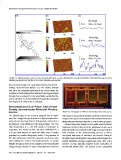
          FIGURE 11. Metal deposition on redox-active molecules attached to a surface: (A) illustration of molecule with top contact; (B) AFM image of surface
          following Ag deposition; (C) profile of the surface following Ag deposition.

          Raman spectroscopy, XPS, cyclic voltammetry, and current
          voltage measurements (Figure 11). The studies indicate
          that all of the porphyrin monolayers are robust under the
          conditions of metal deposition. Neither Cu nor Ag penetrates
          through the monolayer to form electrically conductive fila-
          ments, whereas Au does penetrate through the porphyrin
          monolayer and contacts the Si substrate.

          Demonstration of Low-Power, High Charge
          Density, Semiconductor/Molecular Memory
          Devices                                              FIGURE 12. Photograph of 1 Mb test chip developed by ZettaCore, Inc.
          The ultimate goal of our research program was to imple-  cell is equal to (or greater than) that achieved in trench/stack
          ment the charge-storage molecules in hybrid semiconduc-  designs. This aspect of the hybrid semiconductor/molecular
          tor/molecular memory devices. This goal was achieved in a  design was another key objective of our research program.
                                                       2
          prototypical 1-Mb DRAM test chip design (Figure 12). The  Another important feature of the hybrid semiconductor/
          chip incorporates 4  256 kbit arrays of molecularSi  molecular DRAM is that all of the peripheral circuits were
          capacitors. The circuits on the chip were fabricated on a  fabricated with conventional technology. Consequently, the
          0.35 μm flow process to avoid the high costs of masks  only variation in the manufacturing process is where
          prepared on smaller lithography nodes. A key feature of  the hybrid molecularSi structures are formed. Owing to
          the chip architecture is that the capacitors are planar rather  the high charge density (and consequent planar design), the
          than utilizing the vertical dimension (trenches or stacks).  overall fabrication process requires less than 10% of the
          Despite the planar area of the capacitor, the demonstrated  number of steps typically required in the fabrication of
          charge-storage density in each molecular-based memory  commercial DRAM chips. The process is also compatible


          648 ’ ACCOUNTS OF CHEMICAL RESEARCH ’ 638–650 ’ 2011 ’ Vol. 44, No. 8

